I. Opcode
Nine bits. 512 rows.
91 instructions plus NOP occupy 92 burned rows. The 512-row control ROM leaves the rest unmapped.
 tomato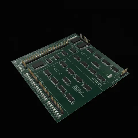
The architecture
I built Tomato around a configurable 32-bit arithmetic and logic engine. Follow an instruction from memory, through the controls and calculation, to the register that keeps the result.
The program counter selects the next 32-bit instruction.
Decode selects the ALU truth tables, immediate format, and data routes.
The register file stores the result; a branch can change what happens next.
Each bit evaluates F and G from A, B and C. The sum combines logic and arithmetic without a final arithmetic-versus-logic output mux.
256 × 256 × 8 controls02 / FEEDThree read ports feed the ALU. One write port stores its result. FPGA stays at 256 × 32-bit registers in eight banks because there is no space for more; r0 is fixed to zero. Discrete is 32,768 and is the primary count.
3 read ports · 1 write port03 / INTERPRETThe immediate box selects among 16 encodings. Instruction overlays reuse bits for constants, register selection and branch controls.
16 immediate selections04 / CONTROLA 9-bit opcode addresses the control ROMs beside each subsystem. The instruction mappings determine which hardware combinations programs can use.
512 control-ROM rows05 / MOVEA barrel shifter, byte-lane memory and program-counter controls complete the datapath around the Dual-LUT.
32-bit words · byte-lane access06 / EXTENDThe working FPGA runs Tomato OS. Broader instruction mappings and compound-operation compiler support develop alongside the remaining discrete boards.
Running FPGA · continuing discrete buildI started with an 8-bit ALU containing 3,488 transistors in total: 624 discrete MOSFETs and 2,864 inside 74HC logic chips. Tomato takes that work into a programmable, 32-bit computer. Its Dual-LUT ALU combines two Boolean functions and carry in one arithmetic operation.
The instruction word, ALU, and register operands are 32 bits wide. Instruction overlays, the immediate box, and the Dual-LUT let me explore how operations map onto the same datapath. The ISA profiles are exploration data: mnemonic and operation comparisons, not implemented decoders, tested foreign binaries, or evidence of native compatibility. Expanding and testing Tomato instruction coverage is part of my software work.
The dual-LUT slice is the center. Matching every LUT pair to its own instruction was never the goal. The 512-row ROM burns what programs need today; the rest of the plane waits in the LUT catalog until a program asks.
The following is the conceptual path shared by the implementations:
Read the next 32-bit instruction.
Select the operands, immediate format, ALU rules and result route.
The Dual-LUT computes; shift and memory paths provide other results.
Store the result. PC control chooses the next instruction address.
Conceptual data flow, not a four-stage pipeline. Control and operand paths operate together.
The program counter fetches from memory into the IR. The register file presents three read ports and accepts one write. ALU control, memory I/O, memory bus, and PC each have their own decode EEPROM—small boards sitting next to the hardware they drive, all listening to the same opcode from the IR. The dual-LUT ALU result returns through the write-back mux on lot 06, not through a cascading 151 tree that would cost tens of nanoseconds per hop.
There is no single linear authority chain. Use the evidence that governs the question: hand-written FPGA RTL for the running FPGA machine; KiCad files, fabrication records, and assembly evidence for physical boards; the burned ROM and ISA tables for instruction encoding; assembler and OS sources for software behavior; and dated journal entries only for what was proposed or observed at that date. Digital schematics are editable design exploration, while exported Verilog is read-only sign-off for that schematic flow.
Compare results and prove the defined ALU properties.
02 / RUNRun the architecture and develop its software.
03 / BUILDTranslate the design into boards, fabricate, solder and bring up.
Instruction mappings in the ISA CSV connect the software to the control ROM. Hardware and software continue together.
alu_out = adder( f(a, b, c), g(a, b, c), carry_in )
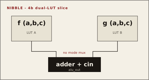
The nibble sliceLUT3 feeds the adder directly. No arithmetic/logic mode mux at the output.
Per nibble, two independent 3-input LUT planes—each a 74ACT151 programmed by an 8-bit opcode bus—sum through a ripple adder. The old topology raced arithmetic and logic into eight 74257 mode muxes at the end of the slice; that branch is gone (why the muxes left). LUT output feeds the adder directly. Carry select uses 74251 muxes; carry-bypass lives inside the 4-bit cell. Every chip gets a 0.1 µF decoupling cap beside it. Toggle the slice in the playground while the first board fills.
Verification ladder: alu-1b-final → 2× alu-4b → 4× alu-8b → alu-32b-final. Lot 07_alu implements one 8-bit slice in copper—99.95×99.80 mm, 25 logic ICs per 8b, soldered and on the bench. Lot 01_alu is the 3,488-transistor predecessor—complete on paper, set aside. The Dual-LUT playground is still the same slice: toggle A, B, C, both opcodes, and carry, then resolve a program from the output you want. Assembly dispatch
Typical packing for ALU register ops. Low bits are often double-booked as immediate or branch overlay, depending on the mnemonic.
| Field | Bits | Slice | Role |
|---|---|---|---|
| Opcode | 9 | [31:23] | Indexes the 512-row microcode ROM |
| rd | 5 | [22:18] | Destination within the selected bank |
| rA / rB / rC | 5 each | [17:3] | ALU operands; rB also imm-high |
| BANK | 3 | [2:0] | Bank select · COND · jump mode |
Native ALU syntax, conceptual: opcode rd, rA, rB, rC — destination is f + g + cin. The architectural register file is 32,768 × 32-bit — that is the primary count, because discrete is the superior design constraint. Thirty-two names times eight banks is the FPGA stand-in: 256 × 32-bit locations, with r0 hardwired to zero, because there is no space for more on that fabric. The current burned ISA addresses that 256-entry array. Low bits double-book as branch condition, jump mode, or immediate overlay depending on the mnemonic—the same slices, different assembly spellings. Field layout authority: opcode-map.csv.
One central microcode blob is elegant in simulation and miserable on a breadboard: twenty-something control wires crawling to the wrong places. Tomato split decode into small boards with local EEPROMs. They all listen to the same opcode from the IR; each sits next to the hardware it drives.
HALT stays on main—opcode plus execute phase, one comparator, not worth its own board. Short ribbons; bring-up in pieces. The master catalog stays the source of truth; a script cuts per-board images. The cost is several EEPROMs instead of one, and opcode fanout to all of them. See the modularization journal for the wiring problem that forced the split.
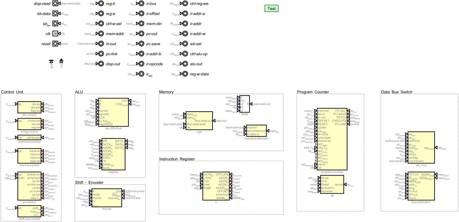
The full datapathDigital schematic: local control boards and the data paths they drive.
Subsystems
Six subsystems, from working storage to the software on screen. Follow each into its board design or build record.
01 · Datapath
Three read ports and one write port serve the FPGA's 256 banked locations — a space-limited stand-in for the discrete 32,768-entry file, which is the primary architectural count. The immediate box supplies constants in 16 formats; the write-back bus selects which result reaches the destination. Register board · Write-back bus
02 · Shift
Priority-encoder multiply on lot 02_shift_encoder: ~4 cycles amortized (worst 16, best zero) vs. ~32 naive add-and-shift. Roughly forty 74ACT157 muxes in the barrel; control on shift-mul-control.
03 · Memory
Lot 03_memory: dual-port RAM, byte-lane decode, 60×80 tile framebuffer. CPU writes tiles; scanout is a separate concern. Timing: load/store pipeline.
04 · Sequencing
Lot 05_program_counter: fetch, branch, jump overlays, interrupts, keyboard vectors, printer I/O. Not video; not TomatoOS.
05 · Video
Tile RAM lives in 03; lot 08_display is scan and panels beyond 07’s bring-up LEDs. FPGA path: polling VPU. Display dispatch.
06 · Firmware
Boot, logo, menu, quirks table, and games — about 2,100 lines of Tomato assembly on tile RAM. Tomato OS sheet
Three facts that do not move
I. Opcode
91 instructions plus NOP occupy 92 burned rows. The 512-row control ROM leaves the rest unmapped.
II. Registers
Discrete is the primary count. FPGA stays at eight banks of 32 because there is no space for more; r0 is hardwired to zero.
III. Authority
FPGA RTL governs the FPGA implementation; KiCad and physical evidence govern boards; ROM/ISA tables govern encoding; software sources govern programs; dated journals govern historical claims.
THE DISCRETE BUILD
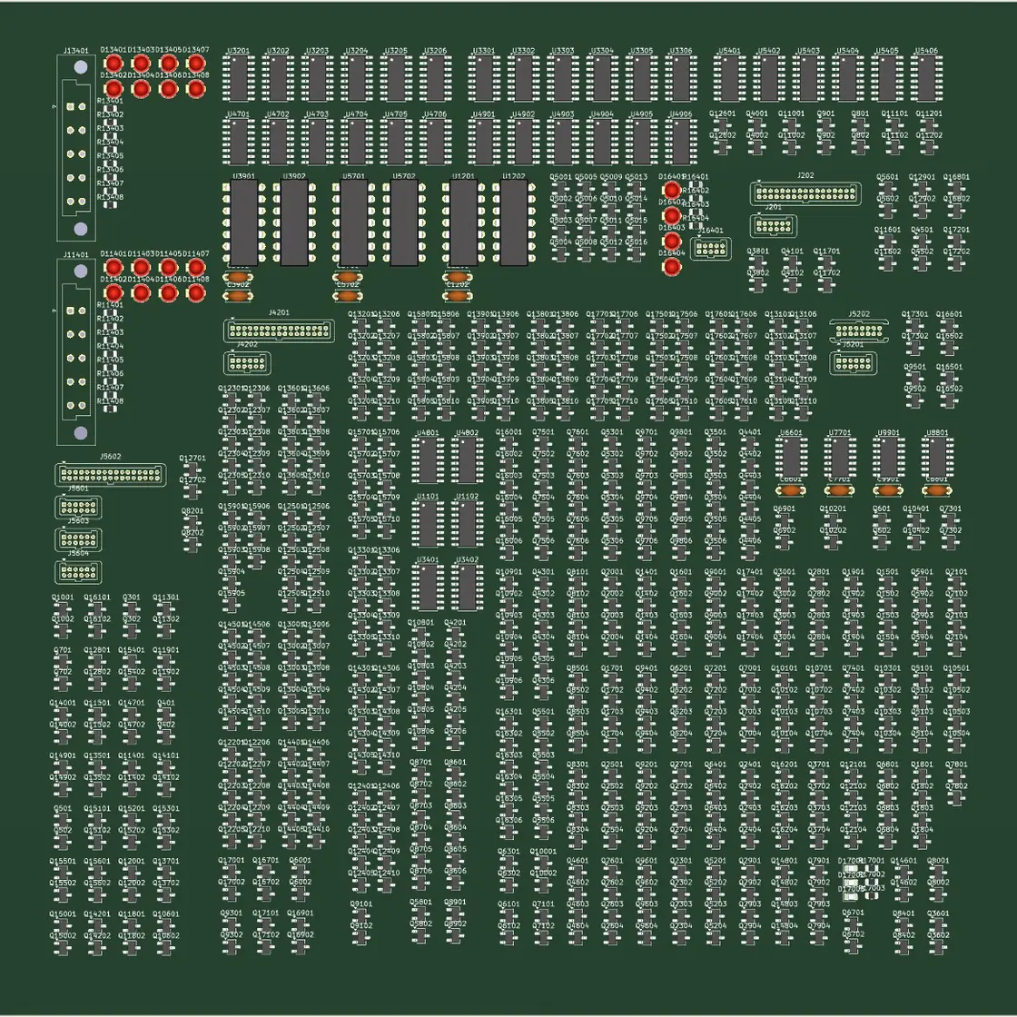 PREDECESSOR · DESIGN RECORD
The transistor-hybrid ALU established the first design. I set it aside before assembly.
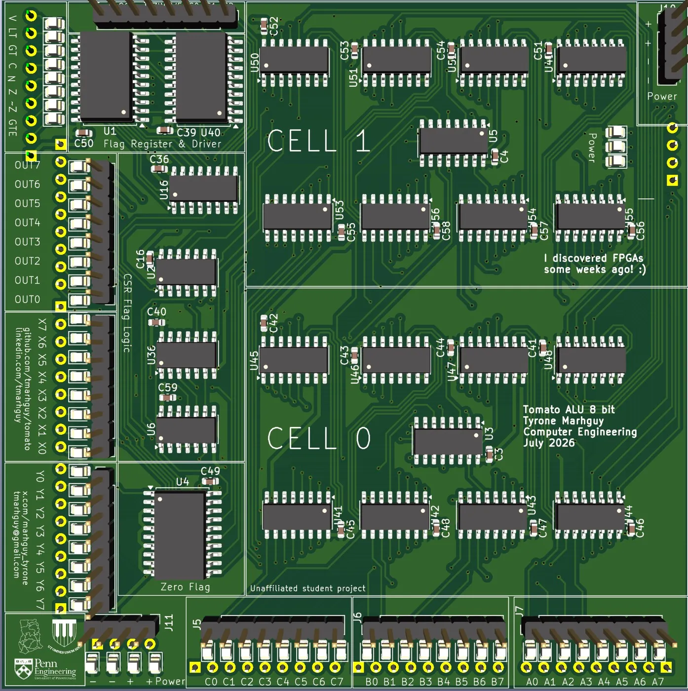 TOMATO · FABRICATED AND SOLDERED
An 8-bit slice in about one-seventh the area. The other discrete subsystems continue alongside FPGA software.
ALU verification
Formal 1b→32b, 476 directed vectors, UVM, and the 10B/130B Verilator gauntlet — the full ladder lives on a dedicated page.
From the build
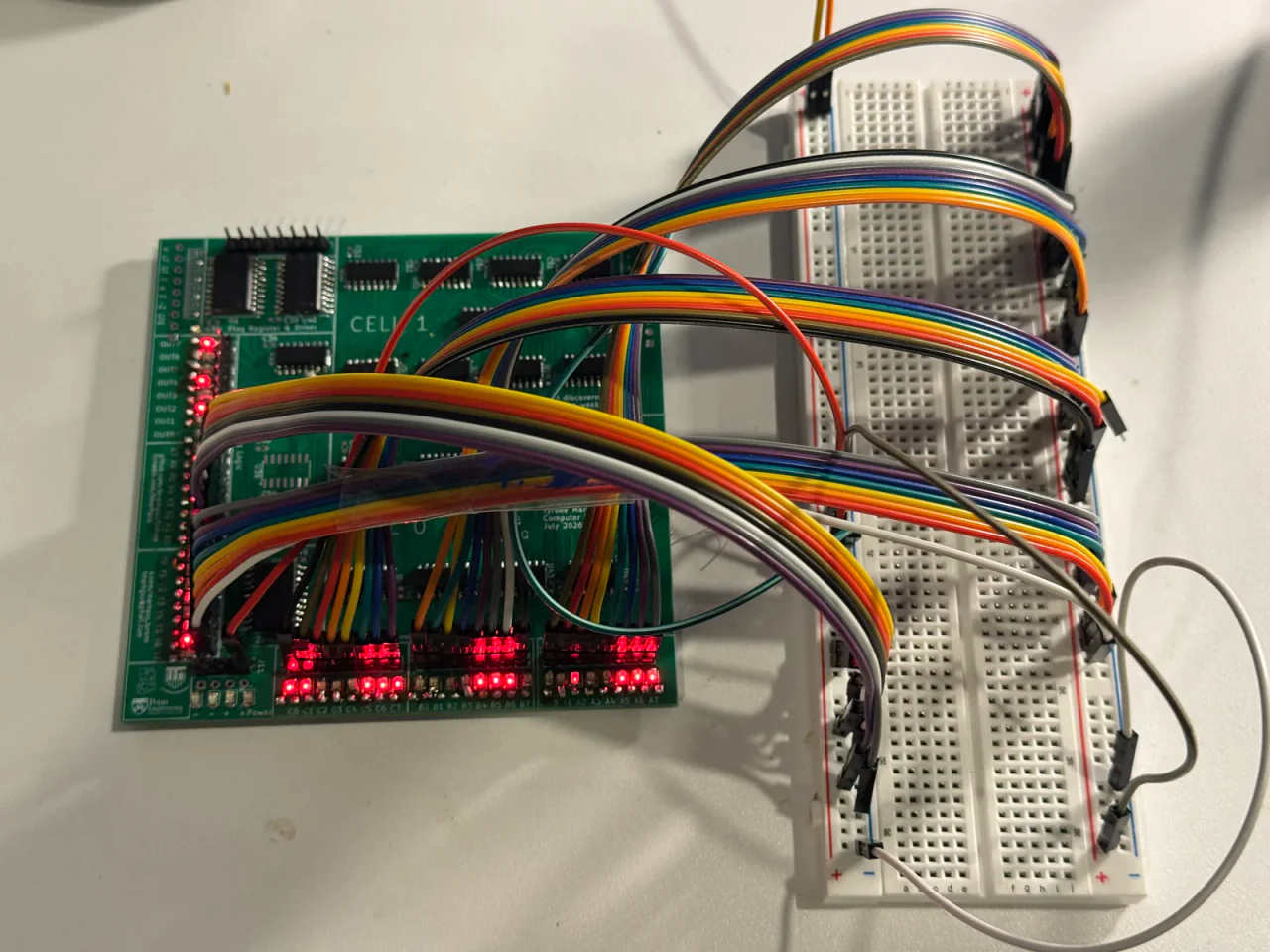
Lot 07 on the bench during board testing.
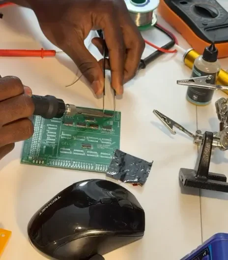
Assembly of the discrete ALU, one package at a time.