
Skip to content
tomato

Dispatch · General Purpose Register File

The address pins were there.
I used all fifteen.

A historical proposal to grow a discrete SRAM register file from 32 to 32,768 locations. Current FPGA RTL uses 256 × 32-bit registers.

Note

More address space. The same instruction width.

This proposal would expose 32,768 32-bit GPR locations because the selected discrete SRAMs (AS6C62256-55PCN, 32K × 8) provide a full 15-bit address space. It describes a proposed mirrored 3R1W discrete structure, not the current FPGA register file.

That is 128 KiB of logical register storage. The comparison with half a Blackwell SM concerns capacity only; it does not compare access behavior or performance.
How the file grew

32 GPR → 256 GPR → 32,768 GPR

  1. 32 GPR register:5
  2. 256 GPR + bank:3
  3. 32,768 GPR + superbank:7

[ superbank:7 ][ bank:3 ][ register:5 ]

7 + 3 + 5 = 15 → 32,768 × 32-bit locations

Historical warning — current context (16 September 2026): this entry records a 32,768-location discrete-memory proposal. Current FPGA RTL implements 256 × 32-bit registers in eight banks, with r0 hardwired to zero. SETBANK2 and the seven-bit superbank are not present in that RTL.

It was only right to start Tomato with the conventional 32 general-purpose registers. But there was an obvious waste: the discrete register file was already going to use parallel asynchronous SRAMs with thousands of available addresses.

Secondary bank is state, not a field

The 7-bit secondary bank is not carried inside every ordinary instruction. It is architectural state. A dedicated custom op changes it:

SETBANK2 · physical address
SETBANK2 0x03          →  superbank_latch ← 0x03
physical_address       =  { superbank_latch, bank, register }

One operation changes the entire visible 256-register window — no copying, no spill to RAM, no widening normal instructions. Ordinary encoding stays:

Instruction word · unchanged width
[ opcode:9 ][ D:5 ][ A:5 ][ B:5 ][ C:5 ][ overlay:3 ]

while the upper seven address bits live in the latch until the next SETBANK2.

Why plain SRAM gives Tomato 3R1W

Tomato's ALU needs three independent register operands, so the file needs three reads and one write. Ordinary async SRAM does not provide that, so the file is mirrored three times.

Four ×8 SRAMs make one 32-bit mirror (4 × (32K × 8) = 32K × 32). Three identical mirrors give the three read ports:

Mirrored 3R1W from twelve chips
Read A Independent address

Mirror A

32K × 32

  • SRAM×8
  • SRAM×8
  • SRAM×8
  • SRAM×8
Read B Independent address

Mirror B

32K × 32

  • SRAM×8
  • SRAM×8
  • SRAM×8
  • SRAM×8
Read C Independent address

Mirror C

32K × 32

  • SRAM×8
  • SRAM×8
  • SRAM×8
  • SRAM×8

Broadcast write

One address + data fan out to every mirror · 1W

4 × (32K × 8) per mirror · 12 AS6C62256 total · effective 3R1W

Writes broadcast address and data to all three; reads present independent addresses. Effective 3R1W from 12 ordinary SRAM chips — no exotic multiported part.

The waste that started this

On an 8K-deep device, 32 architectural registers used 0.39% of the address depth. Tomato's existing 3-bit bank field grew that to 256 GPR — still only 3.125%. The SRAMs, PCB area, 32-bit buses, and three mirrors were already paid for. The unused depth was just sitting there.

SRAM upgrade: AS6C6264 → AS6C62256

Part comparison · same 55 ns class · same 12-chip 3R1W

AS6C6264AS6C62256-55PCN
Organization8K × 832K × 8
Capacity64 Kbit256 Kbit
Address bits1315
32-bit addresses per mirror8,19232,768
Access time55 ns55 ns
Supply2.7–5.5 V2.7–5.5 V
InterfaceAsync parallelAsync parallel
Chips needed for 3R1W1212
Approx. 12-chip cost*~USD 114~USD 122

*Pricing observed during this comparison; distributor and quantity pricing will move.

For roughly USD 7 more across the whole register file: 4× the depth, same chip count, same 55 ns class. So instead of leaving two address lines unused, expose the full device:

Full depth exposed
128 superbanks  ×  8 primary banks  ×  32 registers  =  32,768 GPR

And yes — that number is absurd.

How absurd?

Integer register space · selected architectures

ArchitectureInteger / register space
x86-6416
ARM AArch6431
RISC-V RV32I32
NVIDIA Blackwell255 / thread · 65,536 / SM
Tomato256 / instruction · 32,768

Tomato vs the baselines

BaselineRegister spacevs Tomato
x86-6416 GPR2,048×
RISC-V RV32I32 GPR1,024×
NVIDIA Blackwell SM65,536 × 32-bit physical½ (half)
Tomato256 per instruction · 32,768 in the file

The AS6C62256 presents fifteen address bits; once twelve of those chips are in the BOM for 3R1W, wiring them fully is the only move that isn't waste.

A flat 32K-register ISA would still be terrible: fifteen bits per operand × four → 60 bits just naming registers. Banking keeps the common 5-bit fields and amortizes the upper bits:

Windowed ops after SETBANK2
SETBANK2 0x57

ADD r4, r7, r12
MUL r2, r9, r20
…

All of those ops stay inside the window selected by 0x57 until another bank op changes it. Huge file; ordinary instruction width unchanged.

Final organization

Address map · three reads · one broadcast write
Architectural state

Superbank latch

superbank:7

Normal instruction

15-bit SRAM address

1 of 32,768 GPR

Port map

  • read_A = { superbank, bank, reg_A }
  • read_B = { superbank, bank, reg_B }
  • read_C = { superbank, bank, reg_C }
  • write = { superbank, bank, reg_D } broadcast to all mirrors

256 per instruction window · SETBANK2 moves the superbank field

  1. Add the 7-bit secondary-bank latch and custom SETBANK2
  2. Simulate and test in Hneemann's Digital
  3. Update KiCad register-file / control schematics and SRAM routing
  4. Update the hand-written Verilog / SystemVerilog FPGA core
  5. Test bank switching, isolation, mirrored writes, independent 3R reads, and preservation across superbanks
  6. Run architectural / program regressions
  7. Yosys and the rest of the open-source FPGA flow for hardware bring-up

This proposal started as an attempt not to waste SRAM address pins. It would have exposed 32,768 GPR; current FPGA Tomato instead has 256 × 32-bit registers.

From the build

The work behind the words.

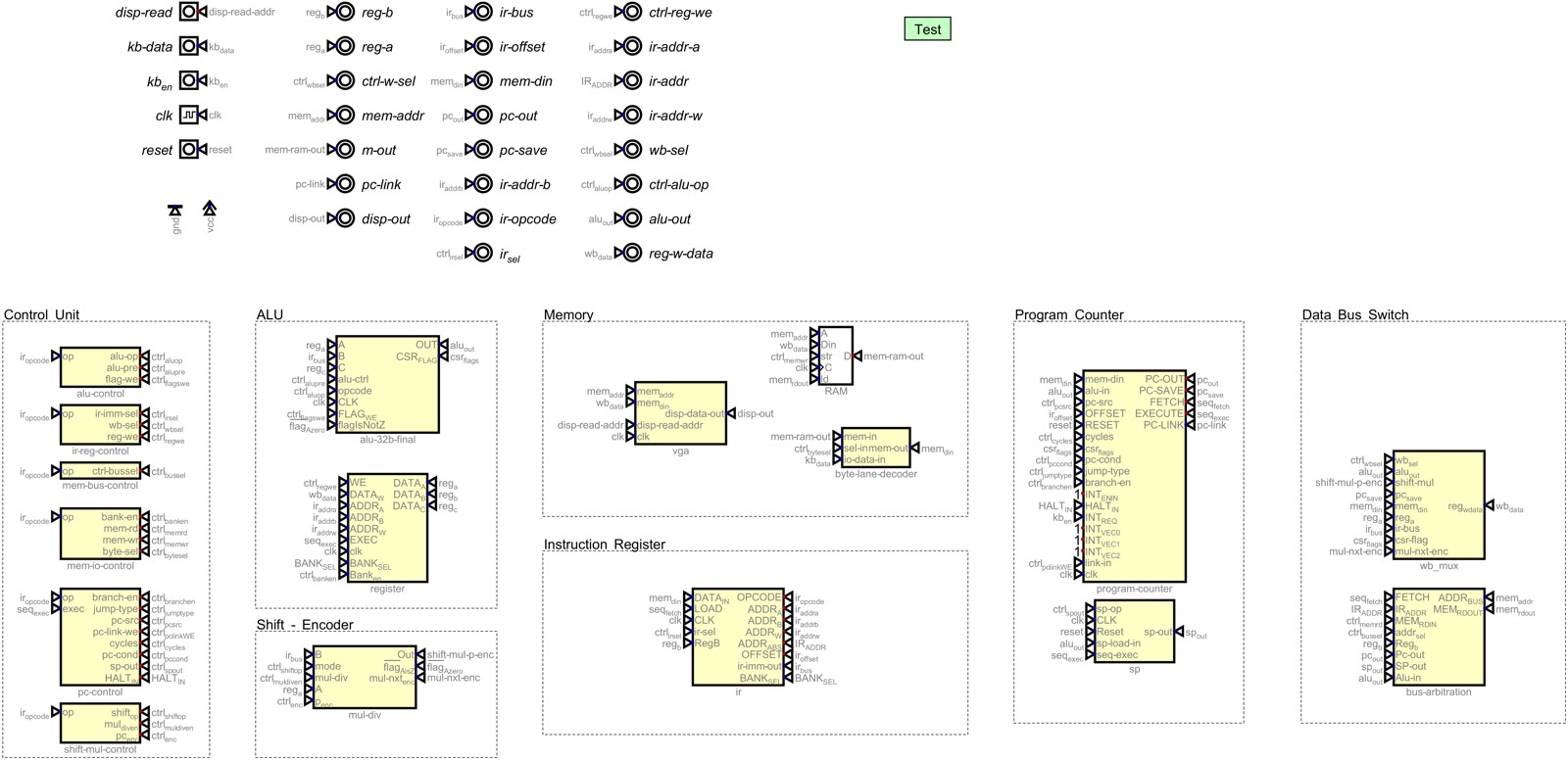
Tomato main schematic in Digital
The complete simulated machine

Datapath and control connected in Digital.

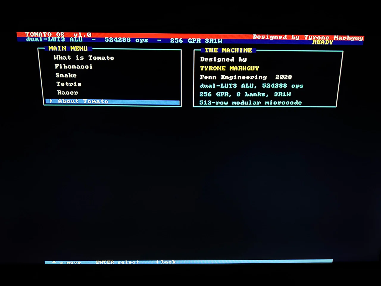
Tomato OS main menu on a display
Tomato OS on screen

The menu running through the FPGA display path.